ST Nucleo WL55JC
Overview
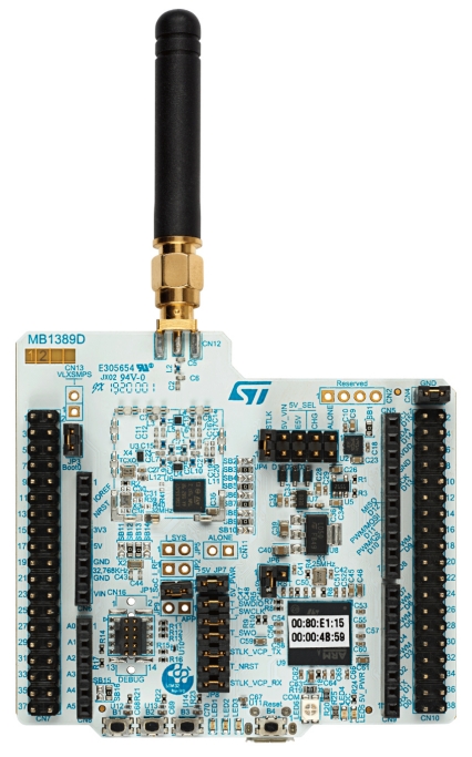
The NUCLEO-WL55JC STM32WL Nucleo-64 board provides an affordable and flexible way for users to try out new concepts and build prototypes with the STM32WL Series microcontroller, choosing from the various combinations of performance, power consumption, and features.
STM32WL55JC microcontroller multiprotocol LPWAN dual-core 32-bit (Arm® Cortex®-M4/M0+ at 48 MHz) in UFBGA73 package featuring:
Ultra-low-power MCU
RF transceiver (150 MHz to 960 MHz frequency range) supporting LoRa®, (G)FSK, (G)MSK, and BPSK modulations
256-Kbyte Flash memory and 64-Kbyte SRAM
3 user LEDs
3 user buttons and 1 reset push-button
32.768 kHz LSE crystal oscillator
32 MHz HSE on-board oscillator
Board connectors:
USB with Micro-B
MIPI debug connector
ARDUINO Uno V3 expansion connector
ST morpho extension pin headers for full access to all STM32WL I/Os
Delivered with SMA antenna
Flexible power-supply options: ST-LINK, USB VBUS, or external sources
On-board STLINK-V3 debugger/programmer with USB re-enumeration capability: mass storage, Virtual COM port, and debug port
Comprehensive free software libraries and examples available with the STM32CubeWL MCU Package
Support of a wide choice of Integrated Development Environments (IDEs) including IAR Embedded Workbench®, MDK-ARM, and STM32CubeIDE
Suitable for rapid prototyping of end nodes based on LoRaWAN, Sigfox, wM-Bus, and many other proprietary protocols
Fully open hardware platform
More information about the board can be found at the Nucleo WL55JC website.
Hardware
The STM32WL55JC long-range wireless and ultra-low-power devices embed a powerful and ultra-low-power LPWAN-compliant radio solution, enabling the following modulations: LoRa®, (G)FSK, (G)MSK, and BPSK It provides the following hardware capabilities:
Radio
Frequency range: 150 MHz to 960 MHz
Modulation: LoRa®, (G)FSK, (G)MSK and BPSK
RX sensitivity: –123 dBm for 2-FSK(at 1.2 Kbit/s), –148 dBm for LoRa® (at 10.4 kHz, spreading factor 12)
Transmitter high output power, programmable up to +22 dBm
Transmitter low output power, programmable up to +15 dBm
Compliant with the following radio frequency regulations such as ETSI EN 300 220, EN 300 113, EN 301 166, FCC CFR 47 Part 15, 24, 90, 101 and the Japanese ARIB STD-T30, T-67, T-108
Compatible with standardized or proprietary protocols such as LoRaWAN®, Sigfox™, W-MBus and more (fully open wireless system-on-chip)
Core
32-bit Arm® Cortex®-M4 CPU
Adaptive real-time accelerator (ART Accelerator) allowing 0-wait-state execution from Flash memory, frequency up to 48 MHz, MPU and DSP instructions
1.25 DMIPS/MHz (Dhrystone 2.1)
32-bit Arm®Cortex®-M0+ CPU
Frequency up to 48 MHz, MPU
0.95 DMIPS/MHz (Dhrystone 2.1)
Security and identification
Hardware encryption AES 256-bit
True random number generator (RNG)
Sector protection against read/write operations (PCROP, RDP, WRP)
CRC calculation unit
Unique device identifier (64-bit UID compliant with IEEE 802-2001 standard)
96-bit unique die identifier
Hardware public key accelerator (PKA)
Key management services
Secure sub-GHz MAC layer
Secure firmware update (SFU)
Secure firmware install (SFI)
Supply and reset management
High-efficiency embedded SMPS step-down converter
SMPS to LDO smart switch
Ultra-safe, low-power BOR (brownout reset) with 5 selectable thresholds
Ultra-low-power POR/PDR
Programmable voltage detector (PVD)
VBAT mode with RTC and 20x32-byte backup registers
Clock sources
32 MHz crystal oscillator
TCXO support: programmable supply voltage
32 kHz oscillator for RTC with calibration
High-speed internal 16 MHz factory trimmed RC (± 1 %)
Internal low-power 32 kHz RC
Internal multi-speed low-power 100 kHz to 48 MHz RC
PLL for CPU, ADC and audio clocks
Memories
256-Kbyte Flash memory
64-Kbyte RAM
20x32-bit backup register
Bootloader supporting USART and SPI interfaces
OTA (over-the-air) firmware update capable
Sector protection against read/write operations
Rich analog peripherals (down to 1.62 V)
12-bit ADC 2.5 Msps, up to 16 bits with hardware oversampling, conversion range up to 3.6 V
12-bit DAC, low-power sample-and-hold
2x ultra-low-power comparators
System peripherals
Mailbox and semaphores for communication between Cortex®-M4 and Cortex®-M0+ firmware
Controllers
2x DMA controller (7 channels each) supporting ADC, DAC, SPI, I2C, LPUART, USART, AES and timers
2x USART (ISO 7816, IrDA, SPI)
1x LPUART (low-power)
2x SPI 16 Mbit/s (1 over 2 supporting I2S)
3x I2C (SMBus/PMBus™)
2x 16-bit 1-channel timer
1x 16-bit 4-channel timer (supporting motor control)
1x 32-bit 4-channel timer
3x 16-bit ultra-low-power timer
1x RTC with 32-bit sub-second wakeup counter
1x independent SysTick
1x independent watchdog
1x window watchdog
Up to 43 I/Os, most 5 V-tolerant
Development support - Serial-wire debug (SWD), JTAG - Dual CPU cross trigger capabilities
More information about STM32WL55JC can be found here:
Supported Features
The Zephyr nucleo_wl55jc board configuration supports the following hardware features:
Interface |
Controller |
Driver/Component |
|---|---|---|
AES |
on-chip |
crypto |
CLOCK |
on-chip |
reset and clock_control |
FLASH |
on-chip |
flash |
GPIO |
on-chip |
gpio |
I2C |
on-chip |
i2c |
MPU |
on-chip |
arch/arm |
NVIC |
on-chip |
arch/arm |
PINMUX |
on-chip |
pinmux |
RADIO |
on-chip |
LoRa |
RNG |
on-chip |
entropy |
SPI |
on-chip |
spi |
UART |
on-chip |
serial port-polling; serial port-interrupt |
Other hardware features are not yet supported on this Zephyr port.
The default configuration can be found in the defconfig and dts files:
Connections and IOs
Nucleo WL55JC Board has 4 GPIO controllers. These controllers are responsible for pin muxing, input/output, pull-up, etc.
Default Zephyr Peripheral Mapping:
LPUART_1 TX/RX : PA3/PA2 (ST-Link Virtual Port Com)
I2C_2_SCL : PA12 (Arduino I2C)
I2C_2_SDA : PA11 (Arduino I2C)
SPI_1_NSS : PA4 (arduino_spi)
SPI_1_SCK : PA5 (arduino_spi)
SPI_1_MISO : PA6 (arduino_spi)
SPI_1_MOSI : PA7 (arduino_spi)
System Clock
Nucleo WL55JC System Clock could be driven by internal or external oscillator, as well as main PLL clock. By default System clock is driven by HSE clock at 32MHz.
Serial Port
Nucleo WL55JC board has 2 (LP)U(S)ARTs. The Zephyr console output is assigned to LPUART_1. Default settings are 115200 8N1.
Programming and Debugging
Applications for the nucleo_wl55jc board configuration can be built the
usual way (see Building an Application).
Flashing
Nucleo WL55JC board includes an STLINK-V3 embedded debug tool
interface. This interface is supported by the openocd version included in the
Zephyr SDK since v0.11.0.
You can also choose the stm32cubeprogrammer runner.
Flashing an application to Nucleo WL55JC
Connect the Nucleo WL55JC to your host computer using the USB port. Then build and flash an application. Here is an example for the Hello World application.
Run a serial host program to connect with your Nucleo board:
$ minicom -D /dev/ttyUSB0
Then build and flash the application.
# From the root of the zephyr repository
west build -b nucleo_wl55jc samples/hello_world
west flash
You should see the following message on the console:
Hello World! arm