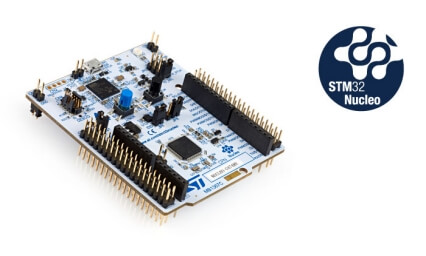
ST Nucleo G474RE
Overview
The Nucleo G474RE board features an ARM Cortex-M4 based STM32G474RE MCU with a wide range of connectivity support and configurations. Here are some highlights of the Nucleo G474RE board:
STM32 microcontroller in LQFP64 package
Arduino Uno V3 connectivity
On-board ST-LINK/V3E debugger/programmer with SWD connector
Flexible board power supply:
USB VBUS or external source(3.3V, 5V, 7 - 12V)
Power management access point
Three LEDs: USB communication (LD1), power LED (LD3), user LED (LD2)
Two push-buttons: RESET and USER
More information about the board can be found at the Nucleo G474RE website.
Hardware
The STM32G474RE SoC provides the following hardware IPs:
Ultra-low-power with FlexPowerControl (down to 28 nA Standby mode and 84 µA/MHz run mode)
Core: ARM® 32-bit Cortex® -M4 CPU with FPU, frequency up to 170 MHz
Clock Sources:
4 to 48 MHz crystal oscillator (HSE)
32 kHz crystal oscillator for RTC (LSE)
Internal 16 MHz factory-trimmed RC ( ±1%)
Internal low-power 32 kHz RC ( ±5%)
2 PLLs for system clock, USB, audio, ADC
RTC with HW calendar, alarms and calibration
14x timers:
1x 32-bit timer and 2x 16-bit timers with up to four IC/OC/PWM or pulse counter and quadrature (incremental) encoder input
2x 16-bit 8-channel advanced motor control timers, with up to 8x PWM channels, dead time generation and emergency stop
1x 16-bit timer with 2x IC/OCs, one OCN/PWM, dead time generation and emergency stop
2x 16-bit timers with IC/OC/OCN/PWM, dead time generation and emergency stop
2x watchdog timers (independent, window)
2x 16-bit basic timers
SysTick timer
1x low-power timer
Up to 86 fast I/Os, most 5 V-tolerant
Memories
Up to 128 KB single bank Flash, proprietary code readout protection
Up to 22 KB of SRAM including 16 KB with hardware parity check
Rich analog peripherals (independent supply)
2x 12-bit ADC 5 MSPS, up to 16-bit with hardware oversampling, 200 µA/MSPS
4x 12-bit DAC, low-power sample and hold
3x operational amplifiers with built-in PGA
4x ultra-fast rail-to-rail analog comparators
16x communication interfaces
1 x FDCAN controller supporting flexible data rate
3x I2C FM+(1 Mbit/s), SMBus/PMBus
4x USARTs (ISO 7816, LIN, IrDA, modem)
1x LPUART
3x SPIs (2x with multiplexed half duplex I2S interface)
1x SAI (serial audio interface)
USB 2.0 full-speed interface with LPM and BCD support
IRTIM (Infrared interface)
USB Type-C™ /USB power delivery controller (UCPD)
12-channel DMA controller
True random number generator (RNG)
CRC calculation unit, 96-bit unique ID
Development support: serial wire debug (SWD), JTAG, Embedded Trace Macrocell*
More information about STM32G474RE can be found here:
Supported Features
The Zephyr nucleo_g474re board configuration supports the following hardware features:
Interface |
Controller |
Driver/Component |
|---|---|---|
NVIC |
on-chip |
nested vector interrupt controller |
UART |
on-chip |
serial port-polling; serial port-interrupt |
PINMUX |
on-chip |
pinmux |
GPIO |
on-chip |
gpio |
I2C |
on-chip |
i2c |
WATCHDOG |
on-chip |
independent watchdog |
PWM |
on-chip |
pwm |
ADC |
on-chip |
adc |
FLASH |
on-chip |
flash memory |
COUNTER |
on-chip |
rtc |
SPI |
on-chip |
spi |
Other hardware features are not yet supported on this Zephyr port.
The default configuration can be found in the defconfig file:
boards/arm/nucleo_g474re/nucleo_g474re_defconfig
Connections and IOs
Nucleo G474RE Board has 6 GPIO controllers. These controllers are responsible for pin muxing, input/output, pull-up, etc.
For mode details please refer to STM32G4 Nucleo-64 board User Manual.
Default Zephyr Peripheral Mapping:
UART_1_TX : PC4
UART_1_RX : PC5
LPUART_1_TX : PA2
LPUART_1_RX : PA3
I2C_1_SCL : PB8
I2C_1_SDA : PB9
SPI_1_NSS : PB6
SPI_1_SCK : PA5
SPI_1_MISO : PA6
SPI_1_MOSI : PA7
SPI_2_NSS : PB12
SPI_2_SCK : PB13
SPI_2_MISO : PB14
SPI_2_MOSI : PB15
SPI_3_NSS : PA15
SPI_3_SCK : PC10
SPI_3_MISO : PC11
SPI_3_MOSI : PC12
PWM_3_CH1 : PB4
USER_PB : PC13
LD2 : PA5
ADC1_IN1 : PA0
System Clock
Nucleo G474RE System Clock could be driven by internal or external oscillator, as well as main PLL clock. By default System clock is driven by PLL clock at 150MHz, driven by 16MHz high speed internal oscillator. The clock can be boosted to 170MHz if boost mode is selected.
Serial Port
Nucleo G474RE board has 3 U(S)ARTs. The Zephyr console output is assigned to LPUART1. Default settings are 115200 8N1.
Please note that LPUART1 baudrate is limited to 9600 if the MCU is clocked by LSE (32.768 kHz) in low power mode.
Programming and Debugging
Applications for the nucleo_g474re board configuration can be built and
flashed in the usual way (see Building an Application and
Run an Application for more details).
Flashing
Nucleo G474RE board includes an ST-LINK/V3E embedded debug tool interface.
Flashing an application to Nucleo G474RE
Connect the Nucleo G474RE to your host computer using the USB port, then run a serial host program to connect with your Nucleo board.
$ minicom -D /dev/ttyACM0
Now build and flash an application. Here is an example for Hello World.
# From the root of the zephyr repository
west build -b nucleo_g474re samples/hello_world
west flash
You should see the following message on the console:
$ Hello World! arm
Debugging
You can debug an application in the usual way. Here is an example for the Hello World application.
# From the root of the zephyr repository
west build -b nucleo_g474re samples/hello_world
west debug